In Santa Clara, the RAM climbed on top of the GPU
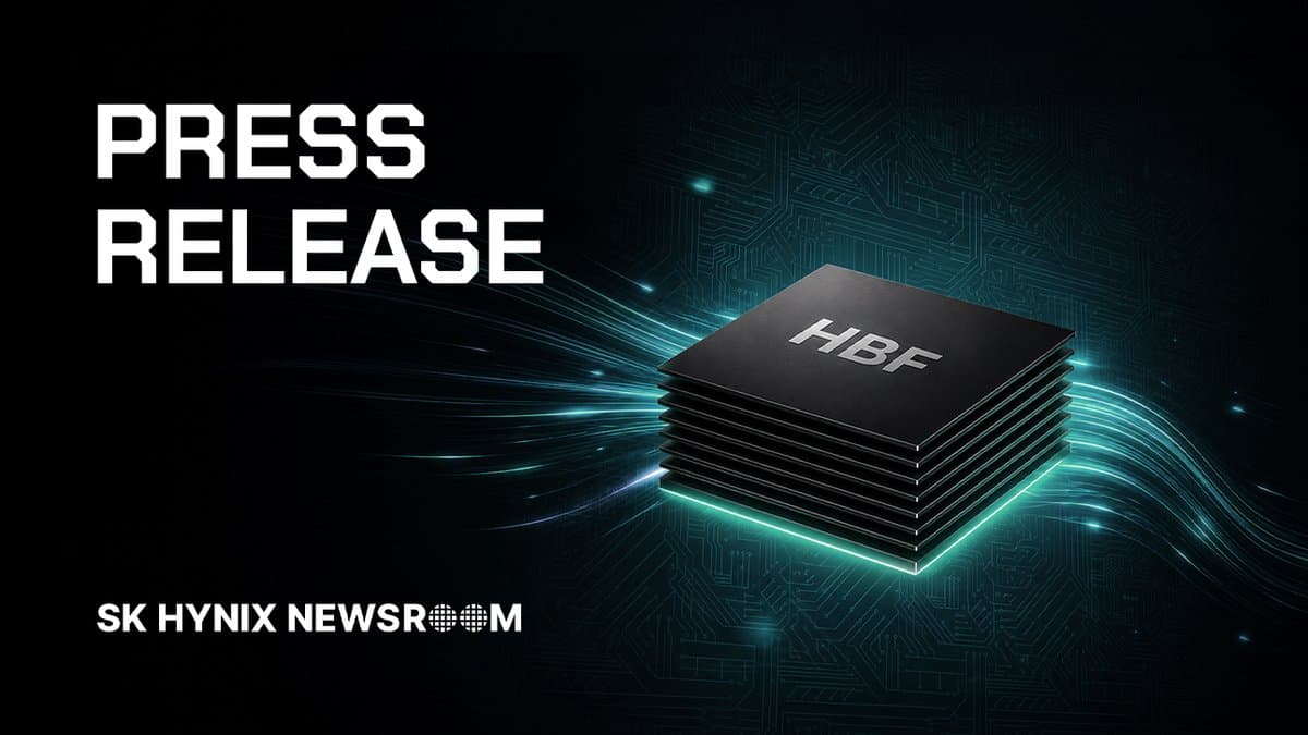
Start with one number: 512GB. That's the capacity of a single stack in the specification SK hynix and Sandisk published on August 4 at the Santa Clara Convention Center. NAND dies piled 8-high or 16-high into one block, half a terabyte per block. And that block doesn't hang off the far end of a PCIe cable like an SSD — it sits next to where HBM sits, wired straight into the accelerator. Bandwidth comes in three grades: roughly 0.4TB/s, 1.5TB/s and 3.0TB/s. The top grade is about a hundred times faster than the fastest PCIe Gen6 SSDs shipping today.
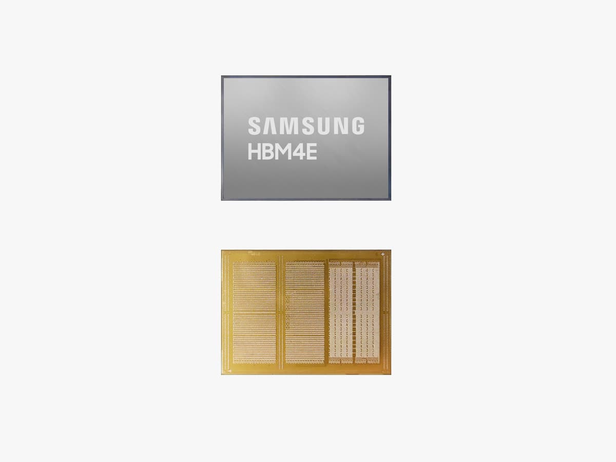
Same day, same show floor, Samsung answered the same question from the opposite direction. Until now HBM has sat beside the GPU die, talking to it across an interposer. Samsung showed a structure that puts it on top of the accelerator instead. It's called zHBM — the "z" being the vertical axis. Samsung's claims: roughly eight times the performance of HBM5, more than ten times the memory density, three times the energy efficiency, and over 50% lower thermal resistance.
The venue was FMS 2026 (Future of Memory and Storage), August 4-6 at the Santa Clara Convention Center. It used to be called the Flash Memory Summit, and a few years ago it was where people argued about SSD controllers and QLC endurance. This year the entire show orbited one question: what are you going to pay for the memory capacity that inference workloads demand?
Here's why that question got urgent. In modern inference serving, the biggest consumer of GPU memory isn't model weights anymore — it's the KV cache, and it grows linearly with conversation length and concurrent users. To borrow The Register's arithmetic, a single 64,000-token sequence on DeepSeek R1 eats about four gigabytes of GPU memory. Put a thousand users in long conversations at once and you're into terabytes just for cache. HBM is too expensive to hold that much. SSDs are cheap enough but far too slow. There's a hole in the middle of the hierarchy, and right now the entire memory industry is aiming at it.
And here's the interesting part: the companies aiming at that hole showed up with different weapons, and they are pointedly not joining each other's camps. The HBF consortium that SK hynix and Sandisk built contains neither Samsung nor Micron nor Kioxia nor Nvidia. This story is mostly about what those absences mean.
Four companies on stage, and the ones who stayed home
Start with SK hynix, because its current condition explains a lot. On July 29 the company reported second-quarter 2026 results: revenue of KRW 79.3187 trillion and operating profit of KRW 60.5426 trillion, an operating margin of 76%. Revenue was up 257% year over year and operating profit up 557%. First-half revenue crossed KRW 100 trillion for the first time in company history. Cash and equivalents hit KRW 88 trillion at quarter-end and the net cash position reached KRW 69.4 trillion. A manufacturing company posting a 76% operating margin is not a sign of a healthy, competitive industry structure — but that is where we are.
Almost all of that profit comes from HBM. Per Counterpoint Research, SK hynix held 58% of the HBM market in Q1 2026, with Samsung and Micron at 21% each — down from 69% in the same quarter a year earlier. UBS expects SK hynix to take roughly 70% of the HBM4 going into Nvidia's next-generation Rubin platform. Translation: SK hynix has already won on the DRAM side, and has not produced an equivalent win on the NAND side. That's the whole reason HBF matters to this company.
Samsung's picture is the mirror image. Samsung was first to mass-produce and ship HBM4, in February 2026; SK hynix didn't start mass production until the second quarter. Counterpoint projects Samsung at 28% and Micron at 18% of the 2026 HBM4 market, which is a meaningfully narrower gap than the overall HBM numbers suggest. And there's one line Samsung kept repeating at FMS: it is the only integrated device manufacturer that owns memory, foundry and advanced packaging under one roof. For something like zHBM — where you have to bond memory directly onto a logic die — that combination is not marketing, it's a prerequisite. A pure memory company physically cannot build this alone.
Samsung's FMS keynote was delivered by Jin-Yub Lee, EVP and Head of Flash Product & Technology, and Kyungryun Kim, VP and Project Leader of the DRAM Design Team. The title was "Driving the Wave of AI Revolution: 3D Innovations in Memory & Storage Architecture." The "3D" wasn't decoration. All three things Samsung brought — zHBM, zNAND-O and V10 BV-NAND — collapse into one sentence: stop spreading out, start stacking up.
The third player is Sandisk, and its position is awkward in an interesting way. Spun out of Western Digital in 2025 and now independently listed, Sandisk co-owns the Japanese fabs in Yokkaichi and Kitakami with Kioxia — the two companies pull NAND off shared wafer lines. Yet Sandisk is pushing HBF with SK hynix while Kioxia does something else entirely. Same fab, two different futures. Sandisk CTO Alper Ilkbahar framed the spec release this way: "AI inference is creating a new set of memory requirements, and HBF technology is designed to meet that moment."
Then there are the two names that joined the consortium during standardization: Google and Tenstorrent. Google designs and deploys its own TPUs. Tenstorrent is Jim Keller's AI accelerator company. Both build accelerators that are not Nvidia's — which is to say, both are companies that have to queue behind Nvidia for HBM allocation. Of course they're interested in a NAND-based capacity tier. And by the same logic, the empty seats tell you as much as the filled ones: Nvidia, AMD, Intel, Broadcom, Qualcomm, Micron and Samsung are all absent.
Eight high, sixteen high, and sixty-four channels
Let's get concrete about what HBF actually is. The specification released through the Open Compute Project is version 0.7.0, and it defines five things: the xPU-HBF host interface, electrical guidelines, baseline performance expectations, reliability and packaging guidance for the HBF die stack, and a software user guide for read and write operations. The "xPU" naming is deliberate — GPU, TPU, NPU, the spec doesn't care.
Physically, it connects over UCIe (Universal Chiplet Interconnect Express), and this is the cleverest design decision in the whole thing. Instead of inventing a new interconnect and begging the industry to adopt it, HBF rides on the chiplet interconnect standard that's already winning. Compare that to HBM, which uses its own dedicated interface. For an accelerator designer, the pitch becomes "if you already have UCIe ports, you can hang HBF off one of them," and that drops the adoption barrier enormously.
Blocks & Files dug into the channel architecture, which explains where 3TB/s comes from. HBF connects through a base controller die exposing up to 16 host channels, each of which can carry one to four AXI channels — up to 64 AXI channels in a maximum configuration. Divide the top 3.072TB/s grade across 64 channels and you get about 49.9 GB/s per channel. For scale: Samsung's PM1763, the PCIe Gen6 SSD that entered mass production in July, does 28.4 GB/s total. Kioxia's first-generation XL-Flash managed 6.2 GB/s across planes. One HBF channel is meant to be faster than an entire flagship SSD.
SK hynix didn't just bring paper. It publicly showed, for the first time, the wafer and products for its tenth-generation (V10) 375-layer 4D NAND. SK hynix's "4D" naming refers to combining Peri Under Cell — putting the peripheral circuitry beneath the cell array — with charge trap flash, which stores charge in an insulating layer. The company says this generation improves performance per watt by 2.5x over its predecessor, and it plans to start mass production of high-performance, high-capacity enterprise SSDs based on it in early 2027. Kim Chun-sung, EVP and Head of Solution Development, put it this way: with AI applications spreading fast, the industry has reached the point where the entire data processing structure has to be redesigned, and HBF is SK hynix's attempt to widen the boundary between memory and storage.
Samsung's announcement is a different animal — it's a concept, not a spec. zHBM uses multi-wafer bonding to stack HBM vertically above the AI accelerator, with an interlayer that can host customer-specific IP. Shortening the physical distance data travels improves bandwidth and power efficiency at the same time, and Samsung claims thermal resistance drops by more than half. But Samsung disclosed no production timeline, no pricing and no customers. The company first floated the zHBM concept at SEMICON Korea in February; FMS 2026 was the first showing of physical concept models.
Alongside it came zNAND-O, aimed at edge AI: V-NAND-based stacks in 4-layer and 8-layer configurations designed to sit next to an NPU, improving space efficiency and latency for devices that process large datasets locally. And V10 BV-NAND, which uses wafer bonding to exceed 400 layers — a 58% density increase over V9, arriving thirteen years after Samsung shipped the first V-NAND in 2013. Put that next to SK hynix's 375 layers and you can see exactly where the layer race stands.
| Announcement | Company | Key specs | Status |
|---|---|---|---|
| HBF standard spec v0.7.0 | SK hynix + Sandisk (via OCP) | 8-high/16-high NAND stacks, up to 512GB per stack, three bandwidth grades at roughly 0.4 / 1.5 / 3.0 TB/s, UCIe interconnect, up to 64 AXI channels | Spec published Aug 3-4, 2026 |
| 375-layer 4D NAND (V10) | SK hynix | 10th generation, 2.5x better performance per watt | Wafer and products shown for the first time; eSSD mass production early 2027 |
| zHBM | Samsung | HBM stacked vertically on top of the accelerator; claimed 8x performance, 10x density, 3x efficiency and >50% lower thermal resistance vs HBM5 | Concept model, no production date |
| zNAND-O | Samsung | 4-layer and 8-layer configurations, NAND for edge AI | Concept model |
| V10 BV-NAND | Samsung | 400+ layers via wafer bonding, +58% density over V9 | Announced |
| GP1 SSD | Kioxia | PCIe 6.0 / NVMe 2.2, up to 10 million random read IOPS at 512B | FMS Best of Show; evaluation samples late 2026 |
Read that table vertically and the hierarchy comes into focus. HBM inside the accelerator package delivers terabytes per second but tops out at tens of gigabytes per stack at brutal cost. Host DRAM is cheaper and bigger but sits across PCIe or NVLink. NVMe SSDs give you terabytes cheaply at tens of gigabytes per second. HBF is aiming at the empty box labeled "HBM-class bandwidth × NAND-class capacity" — a box nobody has successfully filled.
There are things the spec explicitly doesn't cover, though. As StorageReview noted, v0.7.0 leaves out thermal management guidance, per-stack power budgets, error-correction specifics and any production cost estimates. And there's a bigger variable that neither the spec nor the press releases addressed: write endurance. NAND cells have a finite number of program/erase cycles. Put KV cache — data that gets churned on a per-second basis — on NAND and that limit walks straight into the room. Read-dominant workloads (resident model weights, embedding tables, RAG indexes) look great on HBF. Write-heavy caching needs a separate answer, and that answer hasn't been published yet. Worth flagging plainly.
Who actually collects on this
The clearest beneficiary is SK hynix's NAND business. This is a company that dominates DRAM and does not dominate NAND, at a moment when essentially all AI infrastructure budget flows toward DRAM. If HBF takes hold, NAND gets reclassified from "component in an SSD" to "memory attached to an accelerator." Reclassification means repricing. Given the gap between commodity NAND margins and HBM margins, simply having a path to attach an AI premium to NAND dies is worth an enormous option value. That's also why the 375-layer V10 got its first public showing at this exact event — a standard with no product behind it is just paper.
Sandisk needs this more desperately. Post-spinoff, what it owns is fab equity and a brand, in an industry that has always been violently cyclical. HBF is one of very few exits from that cycle, and leading the specification means owning a stake in the IP and controller design that follows. Look at the pace: standardization work with SK hynix started in August 2025, the OCP workstream launched in February 2026, and the first spec landed six months later. That cadence is what urgency looks like.
For Samsung, zHBM is defense and offense stacked on top of each other. Defense, because if a NAND capacity tier succeeds it cannibalizes some of the "just buy more HBM" demand, and Samsung's revenue center of gravity is still DRAM. Offense, because zHBM creates a place where a memory vendor gets to participate in accelerator design. The detail that matters is the interlayer that can carry customer-specific IP — that is custom HBM by another name, and custom means margin. Building it requires logic foundry plus advanced packaging, and exactly one memory company has both in-house.
Google and Tenstorrent have the simplest math of all. Nvidia has first call on HBM supply; everyone building their own accelerator queues behind it. A standardized NAND-based capacity tier lets them run large-context inference while depending less on the constrained resource. And accelerators that only ever run their owner's workloads — TPUs in Google's own datacenters, for example — can adopt an exotic memory tier far more easily than a general-purpose server can, because the operator knows exactly which data is safe to push down the hierarchy.
Some players got a worse deal out of this. SSD vendors, first: if flash moves next to the GPU, the territory that GPUDirect-style storage was claiming shrinks. Second, the CXL camp, which spent years positioning itself as the memory expansion standard and is now watching the largest new demand pool tilt toward UCIe-based near-compute attachment instead. Third, the NAND makers who stayed out of the spec — in standards fights, latecomers always negotiate from a worse position than founders.
And behind all of this sits the price environment. Per TrendForce, conventional DRAM contract prices rose 90-95% quarter over quarter in Q1 2026 and NAND rose 55-60%, with NAND forecast to climb another 70-75% in Q2. When memory gets that expensive, cost per gigabyte becomes the first-order criterion in architecture decisions. HBF's real sales pitch isn't bandwidth — it's how many gigabytes you can park near the accelerator for a given budget — and in this pricing regime that argument lands harder than it ever has.
The graves of HMC and Optane, and the lesson HBM left behind
The memory industry is not attempting "a new tier between HBM and SSD" for the first time. It has failed at this twice, and both failure modes apply directly to HBF.
The first grave belongs to Hybrid Memory Cube. Micron pushed HMC from 2011 onward, and technically it was ahead of HBM in places. But one difference decided everything: HBM was standardized by JEDEC, an independent standards body, while HMC never got past consortium status. Chip designers are extremely reluctant to bet a silicon design on a specification owned by a single-vendor consortium, because if the consortium collapses so does the supply. Micron abandoned HMC in August 2018 and redirected to GDDR6 and HBM. This lesson points straight at HBF. OCP is a genuinely excellent open hardware community, but it is not JEDEC — and right now two of the three largest NAND makers plus Kioxia are outside the spec.
The second grave is Intel Optane. Built on 3D XPoint, it targeted precisely the gap HBF wants: between DRAM and NAND. The specs still read well today — around 350 nanoseconds of latency for PMem modules, endurance rated at 100 drive writes per day, and 512GB per DIMM at a time when DDR4 topped out at 128GB. It didn't sell. The reason was brutally simple: at any given capacity it cost more than NAND and performed worse than DRAM. Customers kept arriving at the same conclusion — for that money, buy more NAND or plug in more DRAM. The DIMM form factor was also tied to Intel CPUs, which kept the ecosystem narrow. Micron exited 3D XPoint in 2021; Intel wound the business down in 2022 and wrote off $559 million of equipment.
The irony is savage. Four years after Optane died, the workload it was built for finally showed up: the KV cache. The Register's July 29 requiem made exactly this point — a memory tier with sub-microsecond latency and enormous write endurance would have been close to ideal for cache offload, and it left the market four years before the market arrived. The would-be successors chasing that slot today — Kioxia's XL-Flash at roughly 60 drive writes per day, Samsung's Z-NAND — don't match Optane's performance envelope. Few stories illustrate better that timing beats technology. And "this time the timing is right" is the single strongest argument the HBF camp has.
To be fair, look at a success too, and the best one is HBM itself. When JEDEC standardized it in 2013 and AMD shipped it on the Fiji GPU in 2015, HBM was an expensive, low-yield specialty memory for graphics cards. In gaming it essentially failed; GDDR won. A decade later that same technology is producing a 76% operating margin for SK hynix. What made the difference? The standard was genuinely open, the generations kept shipping without gaps, and when demand finally appeared the production lines already existed. HBF has satisfied the first condition by publishing through OCP, is just beginning on the second, and is nowhere near the third — samples are targeted for 2026 and production for 2027, but those are stated plans, not committed schedules.
Kioxia declined the invitation
The first counter-move came from Kioxia, and it's a good one: instead of joining HBF, it showed up with a completely different answer and won an award for it. The GP1 series SSD runs PCIe 6.0 with NVMe 2.2 on second-generation XL-Flash, and delivers up to 10 million random read IOPS at 512-byte access. Kioxia calls it the industry's first super-high-IOPS PCIe SSD optimized for GPU direct access; FMS 2026 gave it Best of Show in the specialized storage category. Evaluation samples go to selected customers by the end of 2026, and the roadmap points at 100 million IOPS.
Kioxia's logic is straightforward: rather than bolting a new package onto the accelerator, just make the drive in the existing PCIe slot absurdly fast. The advantages are real — no accelerator redesign required, it drops into servers that exist today, and you don't have to win a standards war. The disadvantage is equally real: the moment you cross PCIe you inherit a bandwidth ceiling, and you will never reach the terabytes-per-second territory HBF is claiming. According to reporting, Kioxia is separately developing its own high-bandwidth flash that stacks up to 32 dies with through-silicon vias to attach to the GPU bus, with Nvidia driving those discussions — but that has not been formally announced and shouldn't be read as settled.
Which produces the strangest picture in this whole story. Kioxia and Sandisk jointly own the Japanese fabs. They share wafer capacity while backing incompatible architectures for the same emerging tier. One set of fabs, two futures. If either architecture wins decisively, the loser ends up part-owning the factory that manufactured its rival's victory.
The second counter-move already exists, and it's Nvidia's. Rubin CPX drops HBM entirely in favor of 128GB of GDDR7 at roughly 2TB/s, purpose-built for long-context inference. Same problem, opposite philosophy: instead of inventing a new memory tier, use the cheap graphics memory that already ships in enormous volume. SemiAnalysis has estimated GDDR7 is around five times more cost-effective than HBM for this role. That goes a long way toward explaining why Nvidia isn't in the HBF consortium. It already has an answer, and its answer doesn't have to wait for a standards process.
The third counter-move is software, and it's the one hardware vendors least like discussing. The cheapest way to solve a KV cache problem is usually not to buy new silicon — it's to manage the cache better. Prefix caching, tiered KV cache offload to host DRAM and NVMe, paged-attention-style memory management: all of these matured rapidly over the past two years and absorb a large share of the pressure. Adopting a new memory tier means redesigning servers; upgrading an inference engine means one deployment. If HBF can't demonstrate a clear advantage over the software tier, it risks becoming the sort of technology that's nice to have and never quite necessary.
The fourth counter-move is Samsung's and Micron's silence itself. Two of the top NAND makers sitting outside the spec means HBF has a long road to genuine industry-standard status. Sometimes the first mover wins a standards fight; just as often the party with the most volume walks in late and flips the table. Whether Samsung is ignoring this tier or quietly preparing to join once it proves out is unknowable right now. Industry forums have speculated that Samsung will eventually enter the HBF race, but the company has confirmed nothing.
So what actually changes
If you run AI infrastructure, there's one thing worth doing this month: decompose what's actually consuming GPU memory in your serving stack. Model weights, KV cache, activations — get the ratio. If KV cache is past half and climbing, the hardware options arriving over the next two to three years become directly relevant to your roadmap. If your workload is weight-dominated with short contexts, neither HBF nor CPX is urgent for you. Skipping this diagnosis is how teams end up buying whatever the vendor deck says.
For enterprise decision-makers, the useful judgment is about timing. HBF's spec just landed at v0.7.0, samples are targeted for 2026 and production for 2027. StorageReview's line captures the industry temperature well: people would like to see HBF hardware in a lab before anyone ships production systems built on it. So changing 2026 procurement on the strength of this announcement is premature. But if you're sketching 2027-2028 datacenter designs right now, you have a legitimate new question for your accelerator vendors: what's your roadmap for a UCIe-attached capacity tier? That single question changes the texture of the conversation.
Investors should separate two very different signals here. The short-term one: SK hynix's 76% operating margin comes from HBM, not HBF, and this announcement will contribute approximately zero to results over the next four to six quarters, because HBF revenue does not yet exist. The structural one: a path just opened for NAND's business character to change. NAND has been a cyclical commodity, which is why it carries low multiples. If NAND dies get reclassified as AI accelerator components, that multiple logic changes. Whether the transition actually happens is something to judge from 2027 production volumes and the identity of the first customer. Today, only the existence of the option has been confirmed.
There's a less-discussed angle worth naming: consumer memory prices. Through 2026, DRAM and NAND contract prices have jumped by double and sometimes triple digits per quarter, and that shrapnel hits everyone from people building gaming PCs to phone manufacturers. Part of why technologies like HBF and zHBM matter is that, if they work, they add inference capacity while consuming less HBM wafer capacity — and an HBM wafer eats the capacity of several conventional DRAM wafers. That's a multi-year effect, though. It does nothing for next year's RAM prices.
Finally, for regular users. Nothing here changes your experience directly. Indirectly, one thing does. The reason AI services advertise million-token context windows while still forgetting the start of long conversations — or charging steeply when you paste in a long document — is mostly this memory economics problem. The cost of maintaining a long context is the cost of KV cache capacity. Bend that cost curve and "AI with a good memory" gets cheap. What happened on this stage is a fight over where that curve goes.
One sentence to compress the whole thing: for three years, AI hardware competition was about how fast you can compute, and Santa Clara in August 2026 showed the question shifting to how cheaply you can park data next to the compute. Samsung's answer is to move the RAM on top of the accelerator. SK hynix's answer is to bolt the NAND to its side. Both could be right, and both could end up buried next to HMC and Optane.
🥄 Three Things You're Probably Wondering
— So what does this mean for me? Nothing immediate. But if you build or operate AI services, your 2027-2028 infrastructure menu just got wider, and the right first step is measuring how much of your GPU memory the KV cache is eating. As a regular user, you're affected only through when long context finally gets cheap.
— Why is this happening now? Because inference overtook training as the driver of memory demand. Training has fixed weight sizes and predictable memory math; inference grows KV cache linearly with concurrent users times conversation length. Layer on 2026 DRAM contract prices jumping over 90% in a single quarter, and "just buy more HBM" stopped being economically viable. The reason to fill the empty tier came from pricing, not from physics.
— Is HBF ahead of zHBM? They're not really comparable. HBF has a published open specification and a physical 375-layer NAND behind it; zHBM is a concept model with no disclosed production date or customer. On concreteness, HBF is clearly further along. But HBF is also a specification that Samsung, Micron, Kioxia and Nvidia all skipped, and in a standards fight that kind of gap is exactly how HMC died. Which side wins won't be knowable until we see 2027 production volumes and the first named customer, so it's too early to call.
Sources
- SK hynix Newsroom — SK hynix Unveils First HBF Standard Specifications with Sandisk, Presenting AI Memory Solutions at 'FMS 2026'
- Sandisk IR — Sandisk and SK hynix Advance Global Standardization of High Bandwidth Flash with Release of First OCP Technical Specification
- Samsung Semiconductor — Samsung Unveils Next-Gen 3D-Memory Vision at FMS 2026, Charting the Future of AI Infrastructure
- Samsung Global Newsroom — Samsung Unveils Next-Gen 3D-Memory Vision at FMS 2026
- Sandisk — Sandisk and SK hynix Begin Global Standardization of High Bandwidth Flash (February 25, 2026)
- Blocks & Files — Getting flash up close and personal to GPUs (HBF channel architecture)
- StorageReview — High Bandwidth Flash Gets Its First Open Spec: 512GB Stacks and Up to 3.0TB/s
- StorageReview — Samsung Outlines 3D Memory Roadmap for AI Infrastructure at FMS 2026
- Tom's Hardware — New HBF spec outlines tech that can give GPUs terabytes of extra memory
- KIOXIA — GP Series Super High IOPS SSD Named 'Best of Show' at FMS 2026
- KIOXIA — Showcases Flash Storage Innovations for the AI Era at FMS 2026
- SK hynix Newsroom — SK hynix Announces 2Q26 Financial Results
- The Register — A requiem for Optane, Intel's KV cache killer that could have eased the RAM price crunch
- The Register — Why Intel killed its Optane memory business (July 2022)
- TrendForce — Samsung Showcases zHBM at FMS 2026, a Next-Gen 3D Memory Architecture
- EE Times Asia — SK hynix, Sandisk Unveil First High Bandwidth Flash Standard at FMS 2026
Numbers and criteria are as of announcement and may change.