Nvidia GTC 2026: Vera Rubin Unveiled — Complete Technical Breakdown
7 new chips, 50 PFLOPS per GPU, 3.6 ExaFLOPS per rack, Groq 3 LPU, $1T order pipeline, autonomous driving partnerships. Everything Jensen Huang announced at GTC 2026, with full specs and context.
"$1 Trillion in Orders Over the Next Two Years"
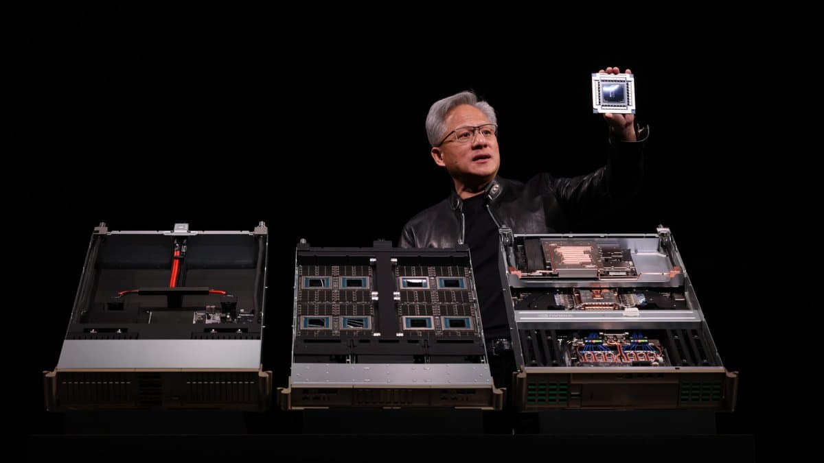
Jensen Huang doesn't do small announcements. At GTC 2026 in San Jose on March 16, he unveiled seven new chips, announced partnerships spanning autonomous vehicles to Disney, and projected a $1 trillion combined order pipeline for Blackwell and Vera Rubin platforms. By any measure, this was the biggest GTC in Nvidia's history.
This article breaks down everything you need to know: the chips, the architectures, the competitive landscape, and what it all means for developers and the broader AI ecosystem.
Background: How We Got Here
To understand Vera Rubin, you need to understand the trajectory. Nvidia's data center GPU evolution has followed an aggressive cadence:
| Generation | Year | Key Innovation |
|---|---|---|
| Volta (V100) | 2017 | First Tensor Cores |
| Ampere (A100) | 2020 | 3rd-gen Tensor Cores, MIG |
| Hopper (H100) | 2022 | Transformer Engine, FP8 |
| Blackwell (B200) | 2024 | 2-die design, FP4, NVLink 5 |
| Vera Rubin (R200) | 2026 | HBM4, NVLink 6, 50 PFLOPS |
Each generation roughly doubles inference performance per watt. Vera Rubin doesn't just double it — Nvidia claims 10x performance per watt over Blackwell for certain AI workloads. How? Three key architectural shifts.
The Rubin GPU (R200) — Full Spec Breakdown
The R200 is a monster. Built on TSMC's N3E (3nm enhanced) process, it packs 336 billion transistors across a multi-die package using TSMC's CoWoS-L (Chip on Wafer on Substrate with Local Silicon Interconnect) technology.
Architecture Details
| Specification | Rubin R200 | Blackwell B200 | Improvement |
|---|---|---|---|
| Process Node | TSMC 3nm (N3E) | TSMC 4nm | ~30% density gain |
| Transistors | 336 billion | 208 billion | 1.6x |
| Die Configuration | 2 compute + 2 I/O chiplets | 2 compute dies | More modular |
| HBM Memory | 288GB HBM4 (8 stacks) | 192GB HBM3e | 1.5x capacity |
| Memory Bandwidth | ~22 TB/s | ~8 TB/s | 2.75x |
| FP4 Inference | 50 PetaFLOPS | ~10 PetaFLOPS | 5x |
| FP8 Training | ~25 PetaFLOPS | ~9 PetaFLOPS | ~2.8x |
| TDP | 2,300W (MaxP) | ~1,200W | — |
| Interconnect | NVLink 6 | NVLink 5 | 2.6x bandwidth |
What Is HBM4 and Why Does It Matter?
HBM (High Bandwidth Memory) is stacked DRAM that sits directly on the GPU package, connected via silicon interposers. Each generation dramatically increases bandwidth:
- HBM2e (A100): 2 TB/s
- HBM3 (H100): 3.35 TB/s
- HBM3e (B200): ~8 TB/s
- HBM4 (R200): ~22 TB/s
HBM4 represents a fundamental architectural change. For the first time, the HBM controller logic moves from the GPU die into the memory stack itself. This means:
- Higher bandwidth without increasing pin count on the GPU
- Better power efficiency — shorter signal paths
- More flexible memory configurations — the GPU can support different HBM4 stack sizes without redesign
For AI inference, memory bandwidth is often the bottleneck. A model like Llama-70B requires ~140GB just for weights in FP16. Generating each token requires reading those weights from memory. More bandwidth = more tokens per second. The jump from 8 TB/s to 22 TB/s means roughly 2.75x faster token generation for memory-bound models.
What Is FP4 and Why 50 PFLOPS?
FP4 (4-bit floating point) is the lowest precision format used in production AI inference. Each number uses just 4 bits instead of 16 (FP16) or 32 (FP32). The tradeoff: lower precision means some accuracy loss, but 4x more operations per clock cycle compared to FP16.
Modern quantization techniques (GPTQ, AWQ, GGUF Q4_K_M) have shown that well-calibrated 4-bit models retain 95-99% of their full-precision quality for most tasks. So 50 PFLOPS of FP4 is not a theoretical number — it's directly applicable to real inference workloads.
Vera CPU — Nvidia's First Custom ARM Processor
This is a bigger deal than most coverage suggests. Nvidia has been using ARM-based Grace CPUs since 2023, but Vera is the first CPU where Nvidia designed the cores from scratch.
- 88 Olympus cores (custom ARM Neoverse-derived)
- Spatial Multithreading: Each core runs 2 threads simultaneously (similar to Intel's Hyper-Threading, but with architectural differences)
- Memory: LPDDR5X, up to 1.2 TB/s bandwidth
- PCIe Gen 6 support
Why does the CPU matter for AI? Because in a full inference pipeline, the CPU handles:
- Tokenization and detokenization
- KV-cache management
- Request scheduling and batching
- Pre/post-processing
A slow CPU creates a bottleneck that no amount of GPU performance can fix. The Vera CPU is specifically designed to keep the R200 GPU fed with work.
NVL72 Rack — Where Theory Meets Reality
Individual GPU specs are impressive, but data centers don't buy individual GPUs. They buy racks. The NVL72 is the actual unit of deployment.
| Specification | Vera Rubin NVL72 | Blackwell NVL72 | Improvement |
|---|---|---|---|
| GPU Count | 72 (36 superchips) | 72 | Same |
| FP4 Inference | 3.6 ExaFLOPS | ~0.9 ExaFLOPS | 4x |
| Total HBM | 20.7 TB | 13.8 TB | 1.5x |
| NVLink Bandwidth | 260 TB/s (NVLink 6) | ~100 TB/s | 2.6x |
| Rack Power | ~190 kW (MaxQ) | ~120 kW | — |
| Cooling | 100% liquid cooling | Hybrid air/liquid | First all-liquid |
| Assembly Time | 18x faster than Blackwell | — | Significant |
3.6 ExaFLOPS from a single rack. To put this in perspective, the world's fastest supercomputer (Frontier at Oak Ridge) achieves about 1.2 ExaFLOPS across 9,408 GPUs filling an entire machine room. A single Vera Rubin NVL72 rack delivers 3x that performance for AI inference workloads.
NVLink 6: The Network Is the Computer
NVLink is Nvidia's proprietary chip-to-chip interconnect. It allows GPUs within a rack to communicate at much higher bandwidth than PCIe.
| NVLink Version | Bandwidth per GPU | Total Rack Bandwidth |
|---|---|---|
| NVLink 4 (Hopper) | 900 GB/s | — |
| NVLink 5 (Blackwell) | 1.8 TB/s | ~100 TB/s |
| NVLink 6 (Vera Rubin) | 3.6 TB/s | 260 TB/s |
This matters for large model training. A 1-trillion-parameter model doesn't fit on a single GPU. It must be split across many GPUs, and they need to constantly exchange data (gradients, activations, KV-cache). Higher NVLink bandwidth means less time waiting for communication and more time computing.
Liquid Cooling: A Paradigm Shift
The Vera Rubin NVL72 is Nvidia's first 100% liquid-cooled rack. This is significant:
- Power efficiency: Liquid cooling uses 30-40% less energy than air cooling for the same thermal load
- Density: No need for large fans and air channels means GPUs can be packed tighter
- Noise: Dramatically quieter operation
- Reliability: Fewer moving parts (fans) means fewer failure points
This signals that future data centers will be fundamentally different from today's air-cooled facilities. Building operators need to plan for liquid cooling infrastructure from the ground up.
Groq 3 LPU — The Biggest Surprise
The most unexpected announcement was Groq 3, the first product from Nvidia's $20B acquisition of Groq in December 2025.
What Is an LPU?
Groq's LPU (Language Processing Unit) is fundamentally different from a GPU. Where GPUs are general-purpose parallel processors, the LPU is a deterministic inference accelerator:
- No HBM at all — uses 500MB of on-chip SRAM instead
- SRAM bandwidth: 150 TB/s — compare to Rubin's HBM4 at 22 TB/s
- 1.2 PetaFLOPS FP8 per LPU
- Deterministic latency — no variable execution paths
Why SRAM Instead of HBM?
SRAM (Static Random Access Memory) is dramatically faster than DRAM (which HBM is based on), but also dramatically more expensive per bit. A single LPU has only 500MB of SRAM vs. the R200's 288GB of HBM4.
The trick is that LPUs aren't meant to hold entire model weights. Instead, they work in a streaming architecture where weights flow through the chip in a deterministic pattern. The result: extreme throughput for inference, but the model must be partitioned across many LPUs.
LPX Rack Configuration
A Groq 3 LPX rack contains 256 LPUs. When paired with a Vera Rubin NVL72:
- Throughput per megawatt: 35x improvement over Vera Rubin alone
- Token latency: Sub-millisecond for small models
- Use case: High-throughput inference serving, real-time applications
Shipping: Q3 2026.
Autonomous Driving — "The ChatGPT Moment Is Here"
Huang dedicated a significant portion of the keynote to autonomous driving, calling it a "ChatGPT moment" for the industry.
New Drive Hyperion Level 4 Partners
- BYD — World's largest EV manufacturer by volume
- Hyundai-Kia — Expanded strategic partnership
- Geely (Volvo parent company)
- Nissan
- Isuzu
Uber Robotaxi Deployment
The most concrete announcement: Uber will deploy Nvidia-powered autonomous vehicles across 28 cities on 4 continents by 2028. The rollout starts in LA and San Francisco in H1 2027.
This is significant because Uber's scale gives Nvidia's autonomous driving platform real-world validation that no other partner can match. Uber handles over 30 million rides per day globally. Even a small fraction of that going autonomous would be transformative.
Developer Ecosystem
CUDA Turns 20
CUDA (Compute Unified Device Architecture) celebrated its 20th anniversary at GTC 2026. Key updates:
- CUDA Toolkit 13.1.1 (January 2026 release)
- Decoupled cuBLAS updates — cuBLAS can now be patched independently without a full CUDA toolkit update
- Nvidia reports over 5 million active CUDA developers worldwide
Agent Toolkit (Open Source)
Nvidia released an open-source Agent Toolkit for building enterprise AI agents. Early adopters include Adobe, Atlassian, Salesforce, SAP, Siemens, ServiceNow, and Red Hat.
NemoClaw
A new open-source stack for developing and deploying long-running AI agents locally. NemoClaw provides:
- Agent orchestration framework
- Memory management for multi-step reasoning
- Tool-use integration
- Local deployment without cloud dependency
DLSS 5 — Beyond Upscaling
DLSS 5 is not an upscaler. It's a "Real-Time Neural Rendering" system that generates complete pixels — including lighting and material interactions — using neural networks. This replaces traditional rasterization for certain rendering tasks. Available for RTX 50 series, launching Fall 2026.
Competitive Landscape
AMD MI400
AMD's response to Blackwell, the MI400 (codename "Antares"), is expected in H2 2026 with:
- TSMC 3nm
- HBM4 support
- ROCm 7.0 software stack
AMD has been gaining traction in inference workloads, but CUDA's 20-year ecosystem advantage remains Nvidia's deepest moat.
Intel Gaudi 3
Intel's Gaudi 3 accelerator targets inference at lower price points. While not competitive with Vera Rubin on absolute performance, Intel is pursuing cost-sensitive enterprise customers.
Custom Silicon
Google (TPU v6), Amazon (Trainium3), and Microsoft (Maia 2) continue developing custom AI chips. These are primarily for internal use and their respective cloud platforms, reducing these hyperscalers' dependence on Nvidia.
Roadmap Through 2028
| Generation | Timing | Key Innovations |
|---|---|---|
| Rubin | H2 2026 | 3nm, HBM4, 50 PFLOPS, NVLink 6 |
| Rubin Ultra | 2027 | 4 compute chiplets, ~100 PFLOPS, 1TB HBM4E |
| Feynman | 2028 | TSMC 1.6nm (A16), 3D die stacking, NVL1152 |
Feynman deserves special attention: it would be Nvidia's first 3D-stacked GPU, and the NVL1152 configuration would put 1,152 GPUs in a single cluster — 16x the current NVL72.
What This Means for Developers
- Inference costs will continue dropping: More efficient hardware means lower cost per token. Plan your pricing models accordingly.
- Liquid cooling is now mandatory: If you're building or leasing data center space, factor in liquid cooling from day one.
- Agent frameworks are going mainstream: Nvidia's investment in NemoClaw and Agent Toolkit signals that autonomous AI agents are the next platform shift.
- The GPU moat is wider than ever: Despite competition, CUDA + NVLink + ecosystem gives Nvidia an advantage that's extremely difficult to replicate.
Key Quotes
"Every SaaS company will become an Agent-as-a-Service company." — Jensen Huang, GTC 2026
"The ChatGPT moment for autonomous driving is here." — Jensen Huang, GTC 2026
"$1 trillion in orders over the next two years — that's what we're looking at." — Jensen Huang, GTC 2026
Competitive Landscape and Background
AMD MI400 vs Nvidia Rubin
AMD has announced the MI400 for H2 2026 — CDNA 5 architecture, TSMC 3nm, HBM4 support. AMD has clawed back ~10% of the AI training market from Nvidia's near-monopoly. But Nvidia's real moat isn't hardware — it's the CUDA ecosystem. Two decades of software stack and developer community can't be replicated overnight.
Intel Falcon Shores — The Quiet Third Player
Intel's AI accelerator Falcon Shores is slated for 2026 shipment, but market reception is tepid. Gaudi 3 underperformed expectations, and there's now talk of Intel spinning off its AI chip business entirely.
The Sovereign AI Race
Another keyword Huang emphasized at GTC: "Sovereign AI." Saudi Arabia, UAE, France, and Japan are building massive domestic AI data centers. This is a core driver of Nvidia's $1T order pipeline. South Korea also announced its national AI computing infrastructure expansion plan in 2026, with KT and SK Telecom adopting Nvidia DGX Cloud.
Historical Context of GPU Computing
Since AlexNet won ImageNet in 2012 using GPUs, GPU has been the core hardware for AI. Nvidia's market cap grew from $10B in 2012 to $4T in 2026 — a 400x increase. Over 95% of that growth is driven by AI demand.
References
관련 기사

NVIDIA GTC 2026: Agentic AI Takes Center Stage, Vera CPU Crushes the Bottleneck
OpenAI Doubles Down on Cerebras: $20B Deal + Equity Warrant
Micron Revenue Nearly Triples to $23.86B — AI Is Creating a Memory Supercycle
AI 트렌드를 앞서가세요
매일 아침, 엄선된 AI 뉴스를 받아보세요. 스팸 없음. 언제든 구독 취소.