AI finally walked into the factory that makes the chips
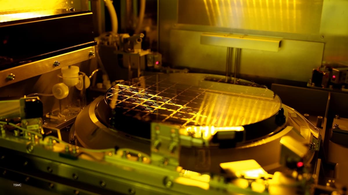
Here's the deal: almost every NVIDIA story so far has pointed one direction — "you need NVIDIA GPUs to run AI." Data centers, training, inference: all about consuming GPUs. But the announcement that dropped June 1, timed to Computex 2026, points the other way. The world's #1 foundry, TSMC, is putting NVIDIA's accelerated computing and AI into the entire process of designing and manufacturing chips. The stage moved from "we sell AI chips" to "we use AI to build chips faster and cheaper."
Why is that a big deal? Chip manufacturing is one of the most complex processes humans have ever built. You draw nanometer-scale patterns with light (lithography), run hundreds of process steps, and a single microscopic defect can scrap an entire wafer. Nudge the speed, yield, or energy efficiency of that process even a little, and the dollars saved are enormous. NVIDIA and TSMC want to embed AI right there — in the making of the thing.
One-line version: NVIDIA built "chips for AI" and sold them. Now it's feeding that AI back into "the factory that makes chips." AI makes the silicon, and the silicon makes stronger AI — one link of that self-reinforcing loop just got officially wired together.
The players — NVIDIA, TSMC, and the 'CUDA-X' libraries
First, NVIDIA. Everyone calls it a GPU company, but its real moat is the software stack that runs on those GPUs: CUDA. The stars of this announcement are all CUDA-based acceleration libraries — cuLitho (lithography), cuEST (electronic-structure / chemistry simulation), and cuML (machine-learning analytics). NVIDIA doesn't just sell chips; it sells the toolkits that make a specific industry's hardest computations run tens of times faster. This time, it brought that toolkit tailored to the chip-making floor.
Next, TSMC. Apple's chips, NVIDIA's own GPUs, AMD's parts — they're all baked in TSMC fabs. The overwhelming majority of the world's advanced silicon passes through this one company. So when TSMC adopts an outside vendor's AI (NVIDIA's) across its full process flow, that's not a casual move. A foundry lives and dies on yield and cycle time, and AI is now touching exactly those levers. For NVIDIA, one of its biggest GPU customers just became a customer of its AI tooling too.
The third player is more abstract but key: the idea that manufacturing problems are computable problems. Lithography correction, defect inspection — these used to crawl along on human experience and CPU math. Redefine them as GPU-accelerated AI problems, and you can do the same work tens of times faster, or far more precisely in the same time. The essence of this partnership is turning manufacturing into a software problem.
What's actually in it — AI planted in six places
NVIDIA named roughly six application points. Walk through them and the picture clicks.
First, lithography. The GPU-accelerated computational-lithography library cuLitho delivers a 20–50% improvement in cost effectiveness or cycle time versus CPU-based methods. Lithography is where light draws circuits onto a wafer, and as nodes shrink, the math to correct for light diffraction explodes. Accelerate it on GPUs and you do the same correction much faster — or more precisely.
Second, transistor and materials design. cuEST (GPU-accelerated electronic-structure simulation) speeds chemistry/materials simulation by ~50× on average. Instead of physically fabricating every new material or transistor structure in a lab, you simulate atomic-scale behavior on a computer and shortlist candidates fast.
Third, process control. The cuML machine-learning library analyzes hundreds of thousands of process parameters at once to cut process variation. A semiconductor process has tens of thousands of variables — temperature, pressure, gas concentration — and AI analysis pinpoints where variation creeps in, lifting yield.
Fourth, fab operations: NVIDIA H200 GPUs plus CUDA-based scheduling manage complex production constraints and optimize routing to raise fab productivity. Fifth, defect inspection: vision AI catches nanometer-scale defects better while cutting repetitive labeling and retraining. Sixth, fab planning: NVIDIA Omniverse builds a virtual fab called "FabTwin," simulating and validating tool layouts digitally before anything is built physically. A single new fab costs tens of billions of dollars — so you run it as a digital twin first.
| Application | NVIDIA tech | Effect |
|---|---|---|
| Lithography | cuLitho | 20–50% better cost/cycle time |
| Materials & transistor design | cuEST | ~50× chemistry-sim speedup |
| Process control | cuML | analyze 100k+ params, cut variation |
| Fab scheduling | H200 GPU + CUDA | optimize production routing |
| Defect inspection | Vision AI | better nanometer-scale detection |
| Fab design/planning | Omniverse 'FabTwin' | digital validation pre-build |
What each side gets — NVIDIA, TSMC, and the whole industry
For NVIDIA, this digs the moat a layer deeper. It already dominates AI silicon, but this extends the CUDA ecosystem into the floor that makes the chips that make AI. Once a top-tier customer like TSMC starts running cuLitho/cuEST/cuML in production, NVIDIA isn't just selling GPUs — it's claiming the seat of "infrastructure software for the semiconductor industry." Tools baked into a process are very hard to rip out.
For TSMC, it can now directly move the KPIs that define a foundry: yield, cycle time, energy efficiency. With the HBM supercycle blowing up demand for advanced fabs, the ability to pull more good die out faster from the same equipment is money and competitiveness. Trim cycle time 20–50% with cuLitho and tame variation with cuML, and the effect lands straight in the quarterly numbers.
For the industry at large, the "software-ization of manufacturing" accelerates. Advanced-node limits have long been a physics problem — wavelength of light, size of atoms. This opens a path to push some of that limit back with "smarter computation." Catch defects faster, find materials faster, design fabs better, and you can keep raising effective productivity even where Moore's Law is physically slowing.
Prior cases — cuLitho isn't actually new
NVIDIA's "AI to accelerate chipmaking" didn't appear from nowhere. History shows both the success and the limits.
Seed of success — the 2023 cuLitho reveal. NVIDIA first unveiled cuLitho at GTC years ago, and even then TSMC, Synopsys, and ASML were named partners. Back then it was close to a single point — "accelerate lithography math on GPUs." What's different now is that it's expanded from that one spot to six: design, materials, process control, inspection, and fab planning. A single experiment matured into full-lifecycle adoption.
A contrast — the history of EDA tools. Look at electronic design automation: Synopsys and Cadence spent decades owning the design stage in software. Once an EDA tool became standard, the whole industry moved on top of it. That's exactly what NVIDIA is after — claiming an EDA-like "essential infrastructure software" seat at the manufacturing stage via CUDA. But as EDA showed, that seat doesn't harden overnight; it takes years of validation and trust.
A warning flag — 'demos and volume are different.' There's a chip-industry adage: "what works in the lab and what ships in volume are two completely different problems." cuLitho's 20–50% and cuEST's 50× are NVIDIA/TSMC figures, and whether they hold on a real volume line is a wait-and-see. Plenty of flashy speedups have been shaved down by the variables of a production environment. So treat this as "direction certain, magnitude TBD."
Counter-plays — Intel, AMD, and the EDA camp
On the same Computex 2026 stage, Intel showed rackscale AI infrastructure, and AMD keeps pushing its AI accelerators. But NVIDIA's move has a different texture. If Intel and AMD compete on "better AI chips," NVIDIA is pulling the process that makes those chips into its own ecosystem. Rivals still fab their chips at foundries like TSMC — and if that foundry's process software runs on NVIDIA CUDA, NVIDIA's leverage spreads on a layer that's separate from raw chip-performance competition.
The EDA and equipment camp is a variable too. Synopsys/Cadence (design) and ASML/Applied Materials (equipment) are each bolting AI onto their domains. As NVIDIA pushes deep with cuLitho/cuML, it's collaboration and competition at once. In fact, cuLitho went the partnership route with ASML and Synopsys from the start — a strategy of laying a "GPU-acceleration layer" on top of them rather than a head-on collision. Whether they embrace NVIDIA GPUs or build their own acceleration stacks is the next thing to watch.
Other foundries — especially Samsung and Intel Foundry — can't sit still. If TSMC lifts yield and cycle time with NVIDIA AI, rivals must match the weapon or differentiate elsewhere. Tellingly, around the same time Samsung is relocating its U.S. HQ to its Texas chip cluster, betting on manufacturing strength. If the "AI-armed fab" becomes the new foundry standard, whoever internalizes these tools fastest and deepest wins.
So what changes — by persona
If you're in semiconductors or hardware, this signals that manufacturing is becoming an ever more compute-intensive industry. A fab's edge will increasingly hinge on "how well you run an AI-acceleration stack," not just equipment and headcount. For process engineers, GPU-accelerated tools like cuLitho/cuML will change how the work is done, and the skill of handling yield/inspection data with AI gets more valuable.
If you invest in AI/infrastructure, you just watched NVIDIA's moat widen from "selling GPUs" to "industrial software." Even if AI-chip demand eventually cools, planting CUDA into chip manufacturing and scientific computing diversifies the revenue mix. And the "AI makes silicon, silicon makes AI" loop is fresh fuel for a longer growth story in this sector.
If you're just tracking the trend, the core point: AI has climbed past making outputs (text, images, code) to making the machines that make those outputs. Semiconductors are the bedrock infrastructure of modern civilization, and AI moving into how that bedrock is produced is symbolic. In an era where Moore's Law is physically slowing, "smarter computation" has started to fill some of that gap.
🥄 Three Things You're Probably Wondering
— Is this NVIDIA selling more GPUs, or something bigger? Bigger. Yes, fab GPUs are GPU sales, but the real move is planting CUDA libraries (cuLitho, cuEST, cuML) into TSMC's production flow. That's a shift from "selling hardware" to "becoming the industry's process software." Tools baked into a fab are sticky — that's a deeper moat than a one-time chip order.
— Are the 20–50% and 50× numbers trustworthy? Treat them as vendor-reported direction, not guaranteed outcomes. They come from NVIDIA/TSMC materials, and the chip industry's own adage is "lab results and volume results are different." The direction (AI accelerating fab work) is solid; the exact magnitude on a real production line is something to verify over the coming quarters.
— Does this help anyone other than NVIDIA and TSMC? Indirectly, yes. If AI lifts yield, cycle time, and energy efficiency, advanced chips can get made faster and cheaper — which eventually flows to everyone who buys silicon. It also pressures rival foundries (Samsung, Intel Foundry) to adopt similar AI tooling, accelerating the whole industry's "software-ization of manufacturing."
— What's the single most important takeaway? AI has moved past making outputs (text, images, code) to making the machines that make those outputs. In an era where Moore's Law is physically slowing, "smarter computation" has started filling part of that gap — and the "AI makes silicon, silicon makes AI" loop just got one link wired together.
References
- NVIDIA and TSMC Bring AI Into Fabs to Advance Semiconductor Design and Manufacturing — NVIDIA Newsroom
- NVIDIA and TSMC Bring AI Into Fabs to Advance Semiconductor Design and Manufacturing — GlobeNewswire
- Computex 2026: Nvidia and TSMC are bringing AI into the fab itself — Electronics360
- NVIDIA cuLitho — Computational Lithography Library (NVIDIA Developer)
- NVIDIA Omniverse — Digital Twin Platform (NVIDIA)