Korea's chip map might stretch south — but it's still at the "review" stage
Here's the deal: on June 8, reports said Samsung Electronics and SK Hynix are reviewing plans to build new AI-semiconductor plants in Korea's southwestern Honam region, an item expected on the government's agenda as early as this month. Let's be clear up front — this is a "review / government-agenda" stage, not a confirmed groundbreaking. No site selection or investment figure has been officially announced. But the direction itself is worth examining.
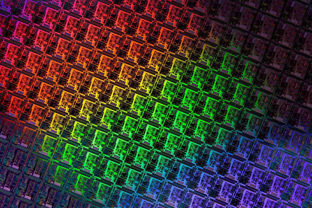
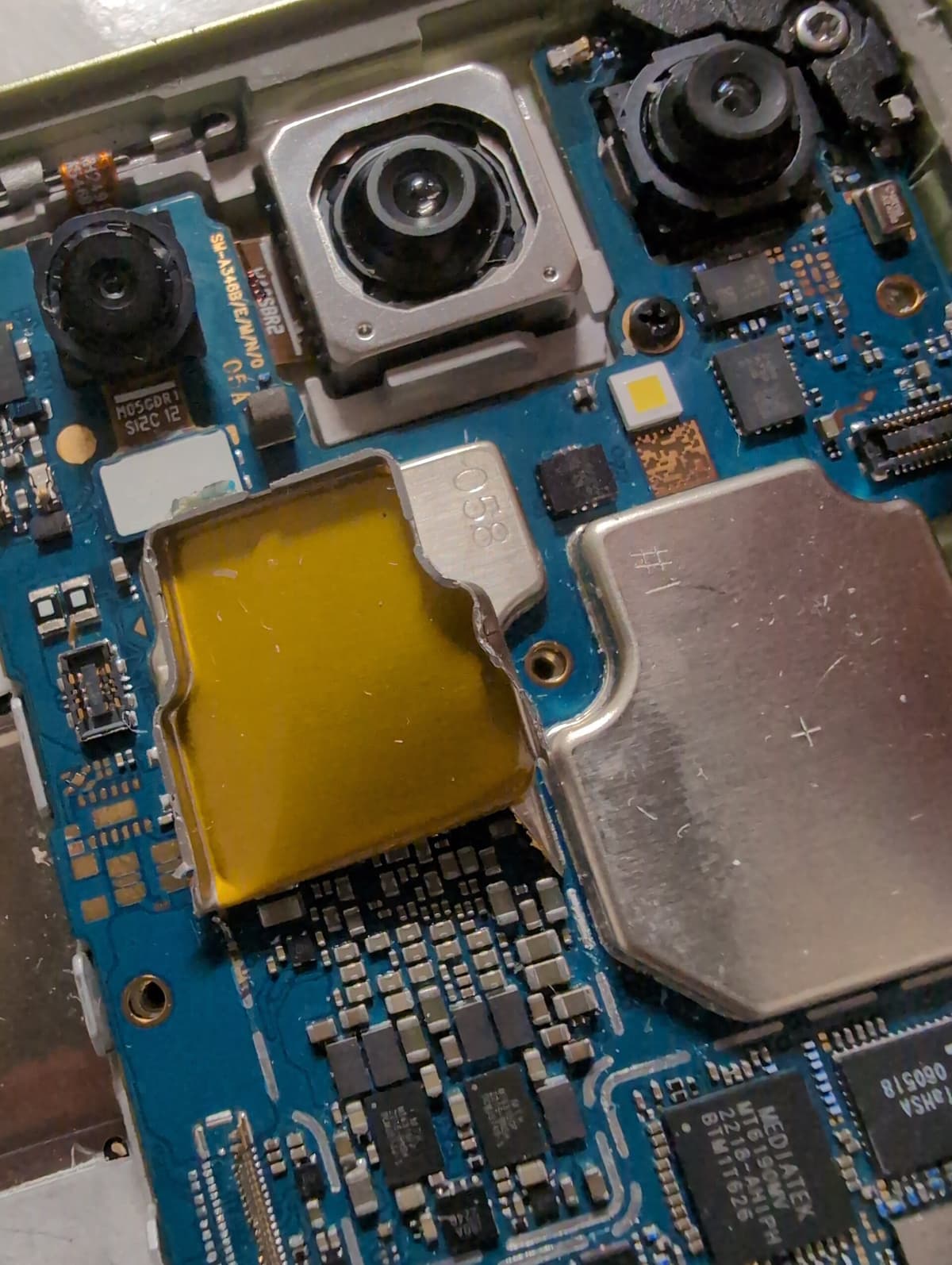
The key point is "what kind of plant." Industry watchers expect advanced-packaging (back-end) plants rather than front-end fabs. That's because the AI-era chip bottleneck has shifted from "how finely you make it" to "how well you bond it" (packaging). Precisely attaching HBM to a GPU and integrating multiple chips into one package — back-end work — is now where the value sits.
Candidate sites include Gwangju, which is freeing up large land by relocating its military airport, and Jangseong County, already developing a data-center complex. With the AI boom making Samsung and SK Hynix trillion-dollar companies and lifting the Kospi ~80%, this reads as part of their broader memory-and-packaging expansion. It's a signal that Korea's chip belt — concentrated around the capital region and Chungcheong — could extend into Honam.
The cast — who's who
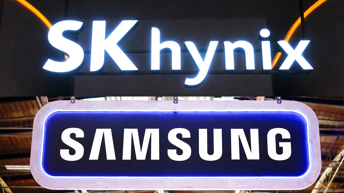
Start with Samsung and SK Hynix, Korea's two semiconductor titans and the AI boom's biggest winners. Both are posting record results on exploding HBM and AI-memory demand, and are aggressively expanding capacity with the proceeds. Their core sites have clustered in Gyeonggi (Giheung, Hwaseong, Pyeongtaek, Icheon) and Chungcheong; this review is novel in that it would stretch that map down to Honam.
The second character is "advanced packaging" itself. Chip competition used to be a miniaturization race — "how many nanometers." But as miniaturization nears physical limits, the new battlefield is "how smartly you stack and bond multiple chips." CoWoS that attaches HBM beside a GPU, 3D stacking that piles chips vertically — all packaging tech. Because it governs AI-chip performance and supply, Samsung and SK want dedicated packaging hubs.
Third are the Korean government and local authorities. The crux is that this is treated as a "government agenda item." AI-chip plants are national industrial strategy, not just corporate investment, so government support (land, power, water, tax) matters. For local governments like Gwangju and Jangseong, landing a big-company chip plant is a regional-economy jackpot, so they're eager to offer sites. Gwangju freeing up land via military-airport relocation is meaningful in this context.
What exactly happened
Let's get the facts straight. Per the June 8 reports, Samsung and SK Hynix are each reviewing new AI-chip plants in Honam, and the matter may reach the government's agenda as early as this month. Industry sees a high chance these are advanced-packaging plants rather than front-end fabs. Candidate sites include Gwangju (the military-airport relocation land) and Jangseong County (developing a data-center complex). To stress again: specifics like investment size and groundbreaking timing aren't official yet.
Why packaging, and why now? Two currents overlap. First, technically, packaging became the AI-chip bottleneck — however well you make a GPU, without bonding HBM you have no finished product, and packaging capacity is globally short. Second, policy-wise, Korea increasingly wants to "internalize packaging beyond memory." Advanced packaging has effectively been led by Taiwan's TSMC, and Korea needs to grow this capability to keep leverage in the AI supply chain.
| Item | Detail |
|---|---|
| Reported | June 8, 2026 |
| Parties | Samsung Electronics, SK Hynix |
| Substance | Reviewing new AI-chip plants in Honam |
| Likely form | Advanced-packaging (back-end) plants (industry view) |
| Candidates | Gwangju (airport-relocation land), Jangseong County (data-center complex) |
| Stage | Review; possible government agenda as early as this month |
| Unconfirmed | Investment size, groundbreaking timing, final site |
| Backdrop | AI boom — both firms ~$1T market cap, Kospi up ~80% |
The table shows it: the big picture (packaging hub, Honam expansion) is set, but the details (money, timing, location) are still in the fog. So read this as "a noteworthy direction," not "a confirmed fact."
What each side gets (if the review becomes real)
For Samsung and SK Hynix, the biggest gain is "securing packaging capacity." As we saw in the SK-TSMC story, SK Hynix partnered with TSMC on base dies and packaging — but long term it must grow its own packaging to keep leverage. Samsung pushes an integrated strategy with memory, foundry, and packaging in-house, so expanding packaging hubs is a core piece of that puzzle. A new Honam hub would also diversify the risk of concentration in one capital-region cluster.
For Honam and its local governments, it's a jackpot. One big-company chip plant brings thousands to tens of thousands of jobs, a supplier ecosystem, and regional tax revenue. Korea's chip investment has concentrated in the capital region and Chungcheong, relatively sidelining Honam; if this review becomes real, it could be a turning point for balanced regional development. Gwangju securing land via airport relocation is a move to seize this chance.
For Korea overall, the gain is "AI supply-chain sovereignty." Shifting from heavy reliance on Taiwan for advanced packaging to growing domestic capability means Korea directly holds more of the AI value chain. Strong in memory (already #1) and now in packaging, Korea's strategic standing rises amid US-China chip tension.
History check — "landing mega-fabs," wins and losses
Chip-plant wins that transformed regions and nations are plentiful. The nearest is Samsung's Pyeongtaek campus. Once empty fields, Pyeongtaek became the world's largest chip complex, drawing jobs and suppliers and reshaping the local economy. The US is similar — TSMC's Arizona fab and Intel's Ohio investment, pushed under the banner of "manufacturing sovereignty in the AI era," are expected to power regional economies. Honam's review extends this "mega-fab transforms a region" success story.
But landing chip plants has traps. First is "time." Review to groundbreaking to operation usually takes years, and if market conditions shift in between, plans get trimmed or delayed. Plenty of global chip investments were announced loudly but slow to break ground. Second is "infrastructure." Advanced chip plants need enormous power and water plus high-skilled talent — whether Honam can supply enough is the question. Land alone doesn't make a plant run.
The core lesson: "review," "groundbreaking," and "operation" are completely different stages. An announcement doesn't mean a plant rises tomorrow — you must climb a long staircase: government agenda → site decision → investment decision → groundbreaking → operation. There are Pyeongtaek-style successes, but also many plans that stalled or shrank. So take this Honam review as "it might begin," not "it's done."
Competitor counter-plays — how do the others respond?
The biggest check is Taiwan's TSMC. As the de facto leader in advanced packaging (CoWoS, etc.), TSMC sees Korea growing its own packaging hub as a long-term threat. Its counter is overwhelming capacity expansion and a technology lead — "you don't need to do it yourself; we package cheaper and faster." Still, the realistic choice for Korean firms is a "two-track" approach like SK Hynix's: cooperate with TSMC while building in-house capability.
The US and Japan's packaging push is a variable too. The US is pouring subsidies into advanced packaging under the AI-supply-chain-localization banner, and Japan eyes an advanced-chip revival via efforts like Rapidus. Korea growing a Honam packaging hub means joining this global "packaging-capacity race." If everyone expands packaging at once, oversupply could loom in a few years — but for now the mood is to grab capacity first.
Inter-regional competition can't be ignored either. Even within Honam, Gwangju and Jangseong are floated as candidates, and other localities covet chip plants. That competition becomes leverage for companies to extract better terms (land, infrastructure, incentives). The final site will hinge on "who best packages power, water, talent, and incentives into an offer."
So what actually changes — by audience
For semiconductor investors, this is news that re-confirms the trend that "AI competition's weight is moving to packaging." That Samsung and SK would even review a Honam packaging hub is evidence that back-end is core to future competitiveness. But this is a "review" stage — not something to price into stocks or earnings now. Track it as it advances through government agenda → site decision → investment decision. Getting ahead of an announcement is risky.
For Honam residents and job seekers, it's worth watching as a potential opportunity — if realized, it brings large-scale jobs and a supplier ecosystem. But since review-to-operation takes years with many variables, it's better to watch progress calmly than inflate expectations now. Distinguishing "what might happen" from "what's confirmed" matters.
For general observers, grab the big picture: "Korean chips are shifting weight toward packaging and trying to stretch geographically south." The next round of the AI-chip war is being fought on packaging, not miniaturization, and Korea is trying to add Honam as a new base on that front. Succeed and Korea's chip footprint widens; stall and it becomes another "loudly announced plan." Right now we're at the mouth of that fork.
🥄 Three Things You're Probably Wondering
— Is building a chip plant in Honam confirmed? No. As of the June 8 reports, it's "under review," with a possible government-agenda discussion as early as this month. Investment size, groundbreaking timing, and final site aren't officially announced. Read it as "direction," not "confirmed."
— Why a packaging plant rather than a front-end fab? Because the AI-era chip bottleneck moved from miniaturization (front-end) to packaging (back-end). However well you make a GPU, without bonding HBM there's no finished product — and packaging capacity is short. So industry sees a high chance the new site is a packaging plant. But that's an observation, not a confirmation.
— Is it decided between Gwangju and Jangseong? Not yet. Gwangju (securing land via airport relocation) and Jangseong County (developing a data-center complex) are floated as candidates. The final site will be decided by power, water, talent, and incentive conditions.
— Why does this matter for Korean chips? First, it's about growing Korea's own capability away from heavy reliance on Taiwan's TSMC for advanced packaging — significant for "AI supply-chain sovereignty." Second, stretching the chip belt from the capital region and Chungcheong into Honam aids balanced regional development. But all of that is contingent on it becoming real.
References
- Samsung and SK Hynix to scale up memory production capacity in 2026 to meet AI demand — Data Center Dynamics
- Samsung and SK Hynix to build new AI semiconductor factories — Sammy Fans
- SK hynix Partners With TSMC to Strengthen HBM Technological Leadership — SK hynix Newsroom
- TrendForce — Korea memory and advanced packaging coverage
- SK hynix to build first U.S. packaging plant for HBM — Tom's Hardware
Numbers and criteria are as of announcement and may change. Investment calls are yours to make!